


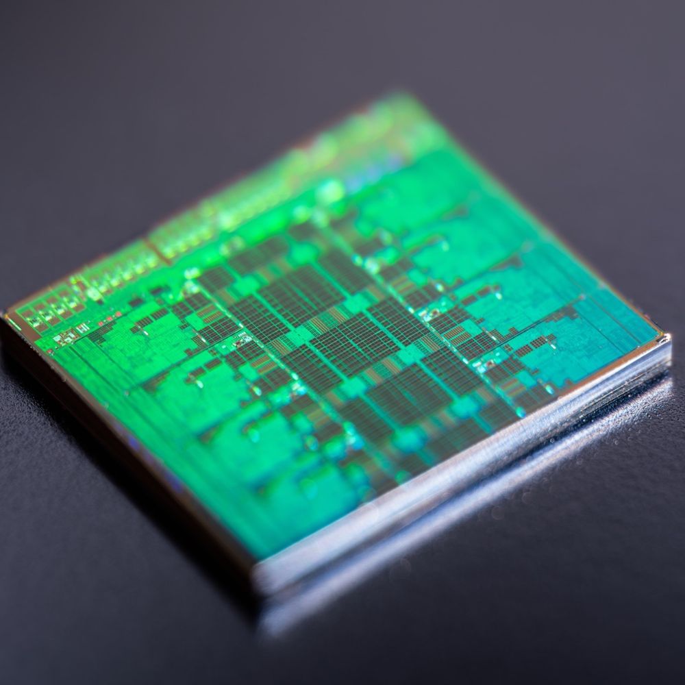
.@awscloud Trainium3
- 3 nm
- 144 GB HBM3E
- 4.9 TB/s
Trn3 UltraServers
- up to 144 Trainium3
- 20.7 TB HBM3E
- 706 TB/s
- NeuronSwitch-v1
- an all-to-all fabric
- 3 nm
- 144 GB HBM3E
- 4.9 TB/s
Trn3 UltraServers
- up to 144 Trainium3
- 20.7 TB HBM3E
- 706 TB/s
- NeuronSwitch-v1
- an all-to-all fabric


December 2, 2025 at 7:08 PM
.@awscloud Trainium3
- 3 nm
- 144 GB HBM3E
- 4.9 TB/s
Trn3 UltraServers
- up to 144 Trainium3
- 20.7 TB HBM3E
- 706 TB/s
- NeuronSwitch-v1
- an all-to-all fabric
- 3 nm
- 144 GB HBM3E
- 4.9 TB/s
Trn3 UltraServers
- up to 144 Trainium3
- 20.7 TB HBM3E
- 706 TB/s
- NeuronSwitch-v1
- an all-to-all fabric
The solvents in some thermal pads seem to dissolve the printing on the GDDR7 memory chips. For a moment, I thought the chips themselves were sticking to them.

December 1, 2025 at 5:38 PM
The solvents in some thermal pads seem to dissolve the printing on the GDDR7 memory chips. For a moment, I thought the chips themselves were sticking to them.
GUC on Integrated Voltage Regulator (IVR) integrated in TSMCs CoWoS-L interposer
GUCs IVR Spec:
- Dual-phase IVR per xPU core or a cluster
- Input voltage: 1.8V
- Programmable output voltage: 0.5V-1.0V
- Efficiency: 85%
- Power density: 3W/mm2
- Can use MIMs and DTCs
GUCs IVR Spec:
- Dual-phase IVR per xPU core or a cluster
- Input voltage: 1.8V
- Programmable output voltage: 0.5V-1.0V
- Efficiency: 85%
- Power density: 3W/mm2
- Can use MIMs and DTCs

November 27, 2025 at 6:27 PM
GUC on Integrated Voltage Regulator (IVR) integrated in TSMCs CoWoS-L interposer
GUCs IVR Spec:
- Dual-phase IVR per xPU core or a cluster
- Input voltage: 1.8V
- Programmable output voltage: 0.5V-1.0V
- Efficiency: 85%
- Power density: 3W/mm2
- Can use MIMs and DTCs
GUCs IVR Spec:
- Dual-phase IVR per xPU core or a cluster
- Input voltage: 1.8V
- Programmable output voltage: 0.5V-1.0V
- Efficiency: 85%
- Power density: 3W/mm2
- Can use MIMs and DTCs
32 GB DDR5-6000 CL30 just 55,998.99 Euros.
It could be a bargain at some point.
It could be a bargain at some point.

November 26, 2025 at 7:22 PM
32 GB DDR5-6000 CL30 just 55,998.99 Euros.
It could be a bargain at some point.
It could be a bargain at some point.
TSMC on HBM4 and C-HBM4E
HBM4:
- N12 base die
- 0.8 V Vdd
C-HBM4E:
- N3P base die
- 0.75 V Vdd
- memory controller inside base die
www.hardwareluxx.de/index.php/ne...
HBM4:
- N12 base die
- 0.8 V Vdd
C-HBM4E:
- N3P base die
- 0.75 V Vdd
- memory controller inside base die
www.hardwareluxx.de/index.php/ne...

November 26, 2025 at 1:59 PM
TSMC on HBM4 and C-HBM4E
HBM4:
- N12 base die
- 0.8 V Vdd
C-HBM4E:
- N3P base die
- 0.75 V Vdd
- memory controller inside base die
www.hardwareluxx.de/index.php/ne...
HBM4:
- N12 base die
- 0.8 V Vdd
C-HBM4E:
- N3P base die
- 0.75 V Vdd
- memory controller inside base die
www.hardwareluxx.de/index.php/ne...
TSMC Advanced Logic Technology Roadmap from OIP Forum Europe – no surprises here. N2P starts in H1 2026. A16 with SPR in H2 2026.
Continuous speed and power scaling, but power/speed shows some slowdown, doesn't it?
www.hardwareluxx.de/index.php/ne...
Continuous speed and power scaling, but power/speed shows some slowdown, doesn't it?
www.hardwareluxx.de/index.php/ne...


November 26, 2025 at 1:41 PM
TSMC Advanced Logic Technology Roadmap from OIP Forum Europe – no surprises here. N2P starts in H1 2026. A16 with SPR in H2 2026.
Continuous speed and power scaling, but power/speed shows some slowdown, doesn't it?
www.hardwareluxx.de/index.php/ne...
Continuous speed and power scaling, but power/speed shows some slowdown, doesn't it?
www.hardwareluxx.de/index.php/ne...
Things are heating up: TSMC formally sues ex-SVP over alleged transfer of secrets to Intel
www.digitimes.com/news/a202511...
www.digitimes.com/news/a202511...
November 25, 2025 at 10:30 AM
Things are heating up: TSMC formally sues ex-SVP over alleged transfer of secrets to Intel
www.digitimes.com/news/a202511...
www.digitimes.com/news/a202511...
I like that kind of stuff. Thats a CFD of the upcoming Artemis II mission that was run on the Cabeus supercomputer. NASA will add two strakes to the core stage of SLS, that will smooth vibrations induced by airflow during ascent - all simulated!
www.youtube.com/watch?v=oJqk...
www.youtube.com/watch?v=oJqk...
November 21, 2025 at 7:56 AM
I like that kind of stuff. Thats a CFD of the upcoming Artemis II mission that was run on the Cabeus supercomputer. NASA will add two strakes to the core stage of SLS, that will smooth vibrations induced by airflow during ascent - all simulated!
www.youtube.com/watch?v=oJqk...
www.youtube.com/watch?v=oJqk...
FP64 is not dead. Do you hear me NVIDIA?
Emulated FP64? Ozaki scheme? Please discuss!
Emulated FP64? Ozaki scheme? Please discuss!

November 19, 2025 at 3:18 PM
FP64 is not dead. Do you hear me NVIDIA?
Emulated FP64? Ozaki scheme? Please discuss!
Emulated FP64? Ozaki scheme? Please discuss!
Microsoft Cobalt 200
- TSMC 3 nm
- two chiplets with custom HB interconnect
- 132 cores (Armv9.2), 66 per chiplet
- 3 MB private L2$
- 192 MB L3$
- 12 memory channels
- per core DVFS
www.hardwareluxx.de/index.php/ne...
- TSMC 3 nm
- two chiplets with custom HB interconnect
- 132 cores (Armv9.2), 66 per chiplet
- 3 MB private L2$
- 192 MB L3$
- 12 memory channels
- per core DVFS
www.hardwareluxx.de/index.php/ne...


November 19, 2025 at 8:29 AM
Microsoft Cobalt 200
- TSMC 3 nm
- two chiplets with custom HB interconnect
- 132 cores (Armv9.2), 66 per chiplet
- 3 MB private L2$
- 192 MB L3$
- 12 memory channels
- per core DVFS
www.hardwareluxx.de/index.php/ne...
- TSMC 3 nm
- two chiplets with custom HB interconnect
- 132 cores (Armv9.2), 66 per chiplet
- 3 MB private L2$
- 192 MB L3$
- 12 memory channels
- per core DVFS
www.hardwareluxx.de/index.php/ne...
Our server needs an upgrade.


November 15, 2025 at 11:31 AM
Our server needs an upgrade.
The DDR5 market goes crazy right now. On the German market, memory kits are sometimes twice as expensive as they were when they were launched a few months ago (or not available at all). This has also led to some memory manufacturers deciding not to launch new series at all.

November 13, 2025 at 12:55 PM
The DDR5 market goes crazy right now. On the German market, memory kits are sometimes twice as expensive as they were when they were launched a few months ago (or not available at all). This has also led to some memory manufacturers deciding not to launch new series at all.
IBM Quantum Loon and Quantum Nighthawk that are being fabricated at NY CREATES' Albany NanoTech Complex on the 300 mm wafer line.


November 13, 2025 at 7:17 AM
IBM Quantum Loon and Quantum Nighthawk that are being fabricated at NY CREATES' Albany NanoTech Complex on the 300 mm wafer line.
"Tachyum Unveils 2nm Prodigy with 21x Higher AI Rack Performance than the Nvidia Rubin Ultra"
- 1,024 64-bit cores
- up to 6 GHz
- 1 GB L2+L3$
- 24x DDR5-17600
- 48 TB per socket
- 128 lanes of PCIe 7.0
- 1,600 W TDP
But surely ...
- 1,024 64-bit cores
- up to 6 GHz
- 1 GB L2+L3$
- 24x DDR5-17600
- 48 TB per socket
- 128 lanes of PCIe 7.0
- 1,600 W TDP
But surely ...

November 12, 2025 at 7:16 PM
"Tachyum Unveils 2nm Prodigy with 21x Higher AI Rack Performance than the Nvidia Rubin Ultra"
- 1,024 64-bit cores
- up to 6 GHz
- 1 GB L2+L3$
- 24x DDR5-17600
- 48 TB per socket
- 128 lanes of PCIe 7.0
- 1,600 W TDP
But surely ...
- 1,024 64-bit cores
- up to 6 GHz
- 1 GB L2+L3$
- 24x DDR5-17600
- 48 TB per socket
- 128 lanes of PCIe 7.0
- 1,600 W TDP
But surely ...
A good addition to the lineup? AMD did today release the Ryzen 5 7500X3D, which is a very efficient six core CPU, but overpriced compared to the Ryzen 5 7600X3D. We are also not sure whether six cores will still be future-proof in 2025.
www.hardwareluxx.de/index.php/ar...
www.hardwareluxx.de/index.php/ar...

November 12, 2025 at 2:46 PM
A good addition to the lineup? AMD did today release the Ryzen 5 7500X3D, which is a very efficient six core CPU, but overpriced compared to the Ryzen 5 7600X3D. We are also not sure whether six cores will still be future-proof in 2025.
www.hardwareluxx.de/index.php/ar...
www.hardwareluxx.de/index.php/ar...
My piece on the Financial Analyst Day by AMD yesterday covering the Zen, Epyc and Instinct roadmaps plus near future product releases and details on them.
www.hardwareluxx.de/index.php/ne...
www.hardwareluxx.de/index.php/ne...


November 12, 2025 at 8:31 AM
My piece on the Financial Analyst Day by AMD yesterday covering the Zen, Epyc and Instinct roadmaps plus near future product releases and details on them.
www.hardwareluxx.de/index.php/ne...
www.hardwareluxx.de/index.php/ne...
Needed to disassemble a GeForce RTX 5090 for a reason. The reason is stupid 🤪


October 31, 2025 at 7:51 PM
Needed to disassemble a GeForce RTX 5090 for a reason. The reason is stupid 🤪
My colleague visited on of the worldwide five pop-up stores by Intel that are or will be located in Munich, Paris, London, New York and Soul.
www.hardwareluxx.de/index.php/ne...
www.hardwareluxx.de/index.php/ne...

October 30, 2025 at 3:44 PM
My colleague visited on of the worldwide five pop-up stores by Intel that are or will be located in Munich, Paris, London, New York and Soul.
www.hardwareluxx.de/index.php/ne...
www.hardwareluxx.de/index.php/ne...
There is a company making billions per quarter, but doing an increasingly bad job in terms of PR. They are giving a lot of infos, also the (in my opinion) important ones, but are holding back on basic stuff like photos of these announcements or are not providing them willingly.
October 29, 2025 at 8:00 AM
There is a company making billions per quarter, but doing an increasingly bad job in terms of PR. They are giving a lot of infos, also the (in my opinion) important ones, but are holding back on basic stuff like photos of these announcements or are not providing them willingly.
This is #Discovery, the next-gen supercomputer run by ORNL and build by HPE. Discovery will use AMD Instinct MI430X accelerators and Epyc "Venice" CPUs.
www.hardwareluxx.de/index.php/ne...
www.hardwareluxx.de/index.php/ne...

October 27, 2025 at 7:16 PM
This is #Discovery, the next-gen supercomputer run by ORNL and build by HPE. Discovery will use AMD Instinct MI430X accelerators and Epyc "Venice" CPUs.
www.hardwareluxx.de/index.php/ne...
www.hardwareluxx.de/index.php/ne...
Single die and dual die implementation of the Maverick-2 by @nextsilicon.com. Single die package is used with the PCIe card while die dual die package sits on the OAM module.


October 25, 2025 at 2:53 PM
Single die and dual die implementation of the Maverick-2 by @nextsilicon.com. Single die package is used with the PCIe card while die dual die package sits on the OAM module.
Die shot from @nextsilicon.com. But this can't be the Maverick-2, because the aspect ratios look a bit strange, or rather, the HBM PHYs are positioned on the long side here. Or am I wrong? It's been a long week, so apologies in advance!

October 24, 2025 at 4:30 PM
Die shot from @nextsilicon.com. But this can't be the Maverick-2, because the aspect ratios look a bit strange, or rather, the HBM PHYs are positioned on the long side here. Or am I wrong? It's been a long week, so apologies in advance!
I‘m kind of shocked that people within the business thought that TSMC manufacturing wafer with Blackwell GPUs in Arizona are giving NVIDIA the ability to do all the silicon related manufacturing independent from Taiwan 🇹🇼
October 21, 2025 at 1:43 PM
I‘m kind of shocked that people within the business thought that TSMC manufacturing wafer with Blackwell GPUs in Arizona are giving NVIDIA the ability to do all the silicon related manufacturing independent from Taiwan 🇹🇼
The two Broadcom #Tomahawk 6 102.4T switch chip in two package variants:
Tomahawk 6 112G SerDes (bigger package)
Tomahawk 6 224G SerDes (smaller package)
Source: @servethehome.com.web.brid.gy
Tomahawk 6 112G SerDes (bigger package)
Tomahawk 6 224G SerDes (smaller package)
Source: @servethehome.com.web.brid.gy


October 20, 2025 at 1:14 PM
The two Broadcom #Tomahawk 6 102.4T switch chip in two package variants:
Tomahawk 6 112G SerDes (bigger package)
Tomahawk 6 224G SerDes (smaller package)
Source: @servethehome.com.web.brid.gy
Tomahawk 6 112G SerDes (bigger package)
Tomahawk 6 224G SerDes (smaller package)
Source: @servethehome.com.web.brid.gy
Researchers at KAUST have stacked six transistors (OxTs and OrTs in an alternating fashion) on top of each other. These stacks consist of 41 layers, fabricated using a 40-step lithography process, each containing 100 devices.

October 20, 2025 at 11:17 AM
Researchers at KAUST have stacked six transistors (OxTs and OrTs in an alternating fashion) on top of each other. These stacks consist of 41 layers, fabricated using a 40-step lithography process, each containing 100 devices.